I/O modules
AXO-005 — LCD1602 character LCD PMOD module
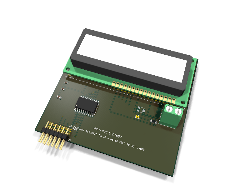
Catalog #5 in the AruviX output line, level L3 (HD44780 parallel 4-bit). A WC1602A 16×2 character LCD (stock symbol and footprint Display:WC1602A verified) running at 5 V from an external screw terminal, with all six host signals buffered up to 5 V.
Circuit review & bench-test guide →
Components#
Every placed component, with the reason it is on the board. Extracted directly from the schematic, so this cannot drift from the design.
| Ref | Value | What it does on this board | Part number | Footprint |
|---|---|---|---|---|
C1 |
100nF 16V X7R | 74AHCT541 supply decoupling | GRM188R71C104KA01DMurata |
C_0603_1608Metric |
C2 |
100nF 16V X7R | LCD VDD decoupling | GRM188R71C104KA01DMurata |
C_0603_1608Metric |
C3 |
10uF 10V X5R | Bulk reservoir on the external 5 V feed (backlight step load) | GRM21BR61A106KE19LMurata |
C_0805_2012Metric |
J1 |
PMOD PLUG 2x6 | PMOD peripheral plug (Digilent spec 1.2) | not selected generic |
PinHeader_2x06_P2.54mm_Horizontal |
J2 |
EXT 5V IN | External 5 V for LCD logic and backlight: 1 +5V, 2 GND (common with PMOD GND) | not selected Phoenix Contact |
TerminalBlock_Phoenix_MKDS-1,5-2-5.08_1x02_P5.08mm_Horizontal |
JP1 |
BACKLIGHT | Backlight enable, bridged by default; cut to kill the backlight (saves ~120 mA) | — | SolderJumper-2_P1.3mm_Bridged_RoundedPad1.0x1.5mm |
R1 |
6.8R | Backlight ballast: (5.0-4.2 V)/120 mA = 6.7 -> 6.8R, ~0.1 W (1206, 0.25 W) | RC1206FR-076R8LYageo Datasheet ↗ |
R_1206_3216Metric |
RV1 |
10k | Contrast trimmer: ends across EXT_5V/GND, wiper to VO | TC33X-2-103EBourns Datasheet ↗ |
Potentiometer_Bourns_TC33X_Vertical |
U1 |
WC1602A | 16x2 character LCD module, HD44780-class controller, 5 V logic | not selected Winstar Datasheet ↗ |
WC1602A |
U2 |
74AHCT541 | Octal 3-state buffer, TTL-threshold inputs (3.3 V -> 5 V level shift) | SN74AHCT541DWTexas Instruments Datasheet ↗ |
SOIC-20W_7.5x12.8mm_P1.27mm |
Signals#
Net labels used in the schematic, which are also the names the HDL top level should use.
3V3 BL_A BL_R D4 D4_5V D5 D5_5V D6 D6_5V D7 D7_5V E EXT_5V E_5V GND RS RS_5V VO
Production status#
| Schematic ERC | 0 violations |
|---|---|
| PCB layout | complete |
| DRC | 0 violations |
| Fab package | exported (24 gerbers + drill + CPL + BOM) |
| Fabricated | no — design stage only |
Source: boards/io-modules/axo-005-lcd1602
Catalog #5 in the AruviX output line (../README.md), level L3 (HD44780 parallel 4-bit). A WC1602A 16×2 character LCD (stock symbol and footprint Display:WC1602A verified) running at 5 V from an external screw terminal, with all six host signals buffered up to 5 V.
Status: schematic generated, ERC clean (0/0), netlist reviewed. PCB layout not started. Not released.
What it teaches#
- The HD44780 init dance (3× function-set, then 4-bit mode) and E-strobed nibble writes as an HDL timing FSM.
- Worst-case-delay design: this board is write-only, so the busy flag is replaced by datasheet timings (>1.52 ms clear/home, >37 µs otherwise).
Design#
- Level shift is mandatory, not optional: HD44780 VIH = 0.7·VDD = 3.5 V at 5 V — host 3.3 V signals are not legal inputs. RS/E/D4–D7 go through a 74AHCT541 (SN74AHCT541DW, SOIC-20W, stock symbol/footprint verified) — one octal buffer covers all 6 lines; the 74AHCT125 alternative would need two packages. A6/A7 grounded, Y6/Y7 open, enables grounded.
- R/W tied to GND (write-only): a read would make the LCD drive 5 V back through D4–D7 — into the 541's outputs (contention) and with no return shifter toward the host. Grounding R/W removes the hazard entirely.
- D0–D3 grounded: unused in 4-bit mode, and with R/W = GND they are always inputs, so grounding is safe.
- Contrast: 10 kΩ trimmer (Bourns TC33X-2-103E, stock footprint verified) across 5 V/GND, wiper → VO.
- Backlight: typical WC1602A LED backlight is ~4.2 V @ 120 mA from 5 V: R = (5.0 − 4.2)/0.12 = 6.7 → 6.8 Ω, P = 0.8 V·0.12 A ≈ 0.1 W → 1206 (0.25 W). JP1 solder jumper (bridged) in series — cut to disable and save ~120 mA.
- 100 nF at the 541 and LCD, 10 µF bulk on the 5 V feed. Extra PWR_FLAG on BL_A (net feeding the backlight power-input pin through the ballast).
| PMOD pin | 1 | 2 | 3 | 4 | 5 | 6 | 7 | 8 | 9 | 10 | 11 | 12 |
|---|---|---|---|---|---|---|---|---|---|---|---|---|
| Net | RS | E | D4 | D5 | GND | 3V3 | D6 | D7 | NC | NC | GND | 3V3 |
External power: J2 pin 1 = +5 V, pin 2 = GND (common with PMOD ground). MPN note: the exact stocked WC1602A variant (backlight color/temperature range) is TBD in the BOM fields.
Regenerate#
python3 generate_design.pyRemaining for release#
- [ ] PCB layout (LCD mounts above the module, 4× M2.5 holes), DRC, fab outputs
- [ ]
hdl/: hd44780 4-bit FSM core + text demo, testbench, ECP5 demo - [ ] BOM export (pin the WC1602A variant), design-review checklist