I/O modules
AXO-010 — Dual waveform DAC (MCP4725 I2C + MCP4822 SPI) PMOD module
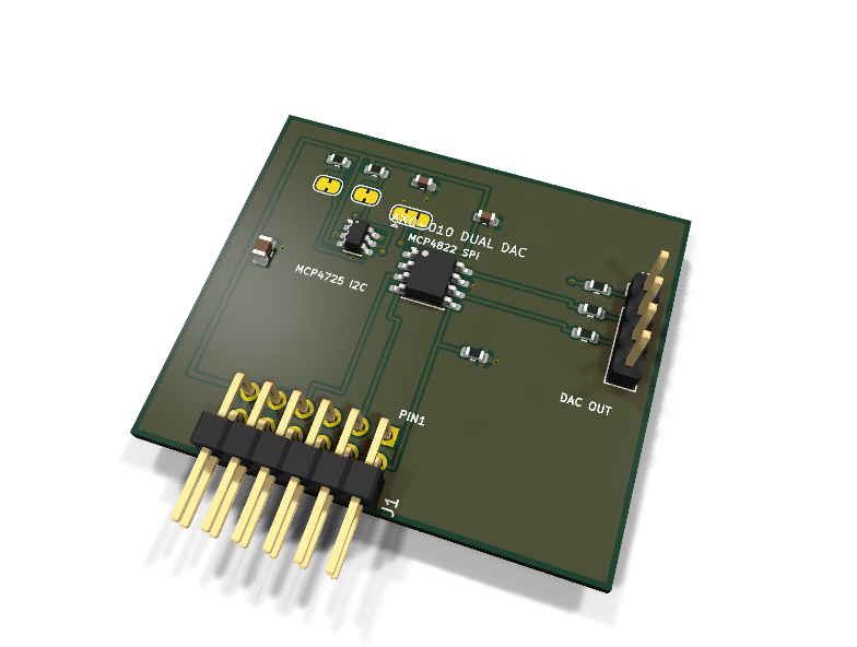
Catalog #10 in the AruviX output line, level L3. BOTH catalog DACs on one board: MCP4725 (12-bit, I2C, EEPROM power-up value) and MCP4822 (dual 12-bit, SPI, internal 2.048 V reference). The DDS/waveform lab — sine tables and phase accumulators in fabric — and the output-side counterpart to the sensor line's ADC modules.
Circuit review & bench-test guide →
Components#
Every placed component, with the reason it is on the board. Extracted directly from the schematic, so this cannot drift from the design.
| Ref | Value | What it does on this board | Part number | Footprint |
|---|---|---|---|---|
C1 |
100nF 16V X7R | MCP4725 supply decoupling | GRM188R71C104KA01DMurata |
C_0603_1608Metric |
C2 |
100nF 16V X7R | MCP4822 supply decoupling | GRM188R71C104KA01DMurata |
C_0603_1608Metric |
C3 |
10uF 10V X5R | Module bulk decoupling (DAC output step loads) | GRM21BR61A106KE19LMurata |
C_0805_2012Metric |
J1 |
PMOD PLUG 2x6 | PMOD peripheral plug (Digilent spec 1.2) | not selected generic |
PinHeader_2x06_P2.54mm_Horizontal |
J2 |
DAC OUT | Waveform outputs: 1 OUT_I2C (MCP4725), 2 OUT_A, 3 OUT_B (MCP4822), 4 GND | not selected generic |
PinHeader_1x04_P2.54mm_Vertical |
JP1 |
SDA PULL-UP | Cut to remove the SDA pull-up when chaining modules | — | SolderJumper-2_P1.3mm_Bridged_RoundedPad1.0x1.5mm |
JP2 |
SCL PULL-UP | Cut to remove the SCL pull-up when chaining modules | — | SolderJumper-2_P1.3mm_Bridged_RoundedPad1.0x1.5mm |
JP3 |
ADDR 0x60/0x61 | MCP4725 address: 1-2 A0 to GND 0x60 (default), 2-3 A0 to VDD 0x61 | — | SolderJumper-3_P1.3mm_Bridged12_RoundedPad1.0x1.5mm |
R1 |
100R | Series isolation on OUT_I2C (op-amp output vs cable capacitance + miswire) | RC0603FR-07100RLYageo Datasheet ↗ |
R_0603_1608Metric |
R2 |
100R | Series isolation on OUT_A (op-amp output vs cable capacitance + miswire) | RC0603FR-07100RLYageo Datasheet ↗ |
R_0603_1608Metric |
R3 |
100R | Series isolation on OUT_B (op-amp output vs cable capacitance + miswire) | RC0603FR-07100RLYageo Datasheet ↗ |
R_0603_1608Metric |
R4 |
4.7k | I2C SDA pull-up | RC0603FR-074K7LYageo Datasheet ↗ |
R_0603_1608Metric |
R5 |
4.7k | I2C SCL pull-up | RC0603FR-074K7LYageo Datasheet ↗ |
R_0603_1608Metric |
R6 |
10k | ~LDAC pull-DOWN: writes latch at ~CS rise by default; host raises then pulses for synchronized A+B update | RC0603FR-0710KLYageo Datasheet ↗ |
R_0603_1608Metric |
U1 |
MCP4725A0 | 12-bit DAC with EEPROM, I2C, VDD-referenced rail-to-rail output | MCP4725A0T-E/CHMicrochip Datasheet ↗ |
SOT-23-6 |
U2 |
MCP4822 | Dual 12-bit DAC, SPI, internal 2.048 V reference, 1x/2x gain | MCP4822-E/SNMicrochip Datasheet ↗ |
SOIC-8_3.9x4.9mm_P1.27mm |
Signals#
Net labels used in the schematic, which are also the names the HDL top level should use.
3V3 A0 CS_N DAC_A DAC_B DAC_I2C GND LDAC_N MOSI OUT_A OUT_B OUT_I2C SCK SCL SCL_PU SDA SDA_PU
Production status#
| Schematic ERC | 0 violations |
|---|---|
| PCB layout | complete |
| DRC | 0 violations |
| Fab package | exported (24 gerbers + drill + CPL + BOM) |
| Fabricated | no — design stage only |
Source: boards/io-modules/axo-010-dac
Catalog #10 in the AruviX output line (../README.md), level L3. BOTH catalog DACs on one board: MCP4725 (12-bit, I2C, EEPROM power-up value) and MCP4822 (dual 12-bit, SPI, internal 2.048 V reference). The DDS/waveform lab — sine tables and phase accumulators in fabric — and the output-side counterpart to the sensor line's ADC modules.
Status: schematic generated, ERC clean (0/0), netlist reviewed. PCB layout not started. Not released.
What it teaches#
Two DAC idioms side by side: the I2C "set a voltage" register model vs the SPI streaming model (20 MHz bus, dds_core phase accumulator + sine ROM). Plus a real datasheet-reading lesson in the ~LDAC latch semantics.
Design#
- MCP4725A0T-E/CH (SOT-23-6, stock symbol
Analog_DAC:MCP4725xxx-xCH); address strap JP3: 1-2 A0→GND = 0x60 (default), 2-3 = 0x61. Standard 4.7 k pull-up jumpers JP1/JP2 on SDA/SCL. - MCP4822-E/SN (SOIC-8, stock symbol
Analog_DAC:MCP4822). Internal 2.048 V reference; note gain=2× aims at 4.096 V full scale but VDD=3.3 V clips near ~3.2 V — use gain=1× for clean waveforms. - ~LDAC is pulled DOWN (10 k), not up — deliberate. Per the MCP4822 datasheet, ~LDAC low makes the output latches transparent, so every SPI write takes effect at the ~CS rising edge. That is the right default for streaming one channel and for hosts that never configure PMOD pin 7. For synchronized A+B updates the host drives pin 7 high, writes both channels, then pulses it low. (A pull-up default would silently freeze the outputs for any host that ignores pin 7.)
- Outputs: MCP4725 VOUT and MCP4822 VOUTA/VOUTB each through 100 Ω to J2 (1×4 header): 1 OUT_I2C, 2 OUT_A, 3 OUT_B, 4 GND.
- 100 nF per DAC + 10 µF bulk, all on PMOD 3V3.
Hybrid PMOD map (documented deviation)#
This board is both SPI and I2C. Instead of squeezing I2C onto top-row pin 3, the I2C bus sits on pins 9/10 — the same bus-repeat positions every AruviX I2C module uses — so the top row stays a clean Type 2 SPI port and I2C chaining conventions are preserved.
| PMOD pin | 1 | 2 | 3 | 4 | 5 | 6 | 7 | 8 | 9 | 10 | 11 | 12 |
|---|---|---|---|---|---|---|---|---|---|---|---|---|
| Net | ~CS | MOSI | NC | SCK | GND | 3V3 | ~LDAC | NC | SCL | SDA | GND | 3V3 |
Regenerate#
python3 generate_design.pyRemaining for release#
- [ ] PCB layout (analog outputs away from SPI clock), DRC, fab outputs
- [ ]
hdl/: dds_core (phase accumulator + sine ROM), SPI/I2C drivers, demo - [ ] BOM export and availability check, design-review checklist