I/O modules
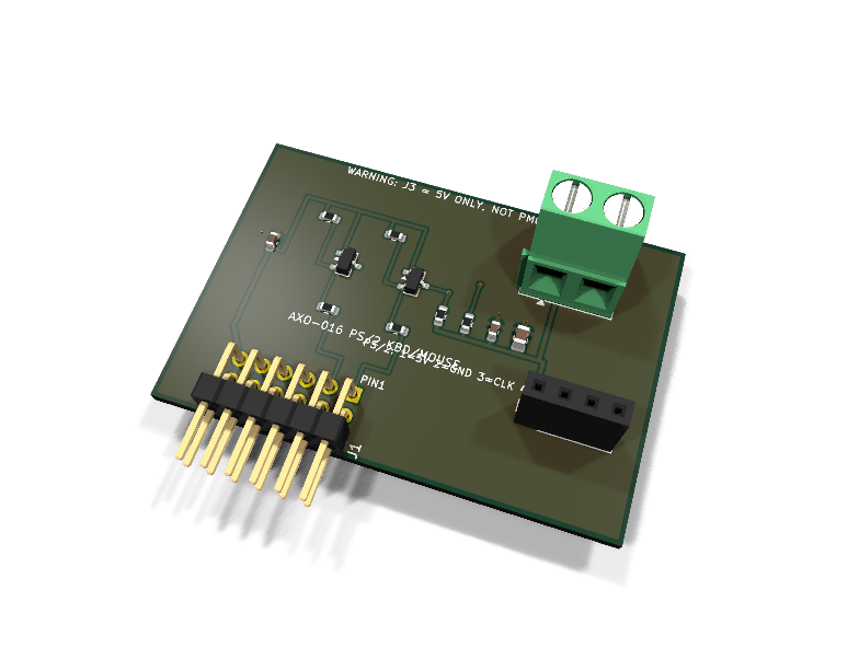
AXO-016 — PS/2 keyboard/mouse PMOD module
Catalog #16 in the AruviX output line, level L3 (PS/2 clock/data protocol). The keyboard keystone of the standalone-computer path: PS/2 in, VGA out, microSD storage — AruviOS with its own keyboard.
Circuit review & bench-test guide →
Components#
Every placed component, with the reason it is on the board. Extracted directly from the schematic, so this cannot drift from the design.
| Ref | Value | What it does on this board | Part number | Footprint |
|---|---|---|---|---|
C1 |
100nF 16V X7R | PS/2 device supply decoupling at the socket | GRM188R71C104KA01DMurata |
C_0603_1608Metric |
C2 |
10uF 10V X5R | Bulk reservoir for keyboard inrush/scan current on the 5 V feed | GRM21BR61A106KE19LMurata |
C_0805_2012Metric |
C3 |
100nF 16V X7R | Module decoupling on the 3.3 V pull-up rail | GRM188R71C104KA01DMurata |
C_0603_1608Metric |
J1 |
PMOD PLUG 2x6 | PMOD peripheral plug (Digilent spec 1.2) | not selected generic |
PinHeader_2x06_P2.54mm_Horizontal |
J2 |
PS/2 PIGTAIL (1x4 SOCKET) | PS/2 pigtail or Mini-DIN-6 panel adapter: 1 +5V, 2 GND, 3 CLK, 4 DATA (5 V side) | not selected generic |
PinSocket_1x04_P2.54mm_Vertical |
J3 |
EXT 5V IN | External 5 V for the PS/2 device: 1 +5V, 2 GND (common with PMOD GND) | not selected Phoenix Contact |
TerminalBlock_Phoenix_MKDS-1,5-2-5.08_1x02_P5.08mm_Horizontal |
Q1 |
BSS138 | Bidirectional open-collector level shifter, PS/2 CLK line | BSS138onsemi Datasheet ↗ |
SOT-23 |
Q2 |
BSS138 | Bidirectional open-collector level shifter, PS/2 DATA line | BSS138onsemi Datasheet ↗ |
SOT-23 |
R1 |
10k | CLK pull-up, 3.3 V side | RC0603FR-0710KLYageo Datasheet ↗ |
R_0603_1608Metric |
R2 |
10k | CLK pull-up, 5 V side | RC0603FR-0710KLYageo Datasheet ↗ |
R_0603_1608Metric |
R3 |
10k | DATA pull-up, 3.3 V side | RC0603FR-0710KLYageo Datasheet ↗ |
R_0603_1608Metric |
R4 |
10k | DATA pull-up, 5 V side | RC0603FR-0710KLYageo Datasheet ↗ |
R_0603_1608Metric |
R5 |
100R | Series protection on the device-driven CLK line | RC0603FR-07100RLYageo Datasheet ↗ |
R_0603_1608Metric |
R6 |
100R | Series protection on the bidirectional DATA line | RC0603FR-07100RLYageo Datasheet ↗ |
R_0603_1608Metric |
Signals#
Net labels used in the schematic, which are also the names the HDL top level should use.
3V3 EXT_5V GND PS2_CLK PS2_CLK_HV PS2_CLK_LV PS2_DATA PS2_DATA_HV PS2_DATA_LV
Production status#
| Schematic ERC | 0 violations |
|---|---|
| PCB layout | complete |
| DRC | 0 violations |
| Fab package | exported (24 gerbers + drill + CPL + BOM) |
| Fabricated | no — design stage only |
Source: boards/io-modules/axo-016-ps2
Catalog #16 in the AruviX output line (../README.md), level L3 (PS/2 clock/data protocol). The keyboard keystone of the standalone-computer path: PS/2 in, VGA out, microSD storage — AruviOS with its own keyboard.
Status: schematic generated, ERC clean (0/0), netlist reviewed. PCB layout not started. Not released.
What it teaches#
The first "real peripheral": PS/2 is open-collector, device-clocked, and slow (10–16.7 kHz) — ideal for a first serial-protocol receiver. Frames are 11 bits: start, 8 data LSB-first, odd parity, stop; the host samples DATA on the falling edge of the device-driven CLK. HDL: instantiate the ps2_rx core from hdl/ (scan-code decode, then a keymap ROM, then an AruviOS keyboard driver).
Design#
- Connector fallback (documented deviation): the stock
Connector:Mini-DIN-6symbol exists, but KiCad 9 ships no Mini-DIN footprint in any library —Connector_DIN.prettyholds only DIN 41612 backplane parts, and a full-library search finds no MiniDIN geometry. Per the never-invent-geometry rule, J2 is a 1x04 2.54 mm socket for a PS/2 pigtail or panel-mount Mini-DIN-6 adapter: 1 VCC(5 V), 2 GND, 3 CLK, 4 DATA. A rev can move to a real Mini-DIN-6 once a verified footprint exists. - 5 V open-collector bus, 3.3 V PMOD: each line gets the classic BSS138 bidirectional shifter (gate to 3V3, source on the 3.3 V side, drain on the 5 V side) with a 10 k pull-up on each side (R1–R4). Open-collector in both directions — needed because the host also transmits (LED/typematic commands) by pulling the lines low.
- External 5 V power (line pattern, like the axs-024 lidar carrier): most keyboards need 5 V at up to ~100 mA, so keyboard power comes from the J3 screw terminal, never the PMOD. Some keyboards do run at 3.3 V — device specific, not relied on. J3 GND is common with the PMOD ground.
- Device-driven lines pass 100 R series resistors (R5/R6) per the line rule; 10 µF + 100 nF on the 5 V feed, 100 nF on the 3.3 V pull-up rail.
- ESD: a hot-plugged, human-touched connector. Rev-A layout should add a TVS array (PESD5V0 class) on CLK/DATA/5V at J2; the host-side PMOD ESD diodes protect the FPGA, not this module's 5 V side.
| PMOD pin | 1 | 2 | 3 | 4 | 5 | 6 | 7 | 8 | 9 | 10 | 11 | 12 |
|---|---|---|---|---|---|---|---|---|---|---|---|---|
| Net | PS2_CLK | PS2_DATA | NC | NC | GND | 3V3 | NC | NC | NC | NC | GND | 3V3 |
Drive rule: open-collector only — pull low or release; never drive high.
Regenerate#
python3 generate_design.pyRemaining for release#
- [ ] PCB layout (J2/J3 on the far edge, TVS array added), DRC, fab outputs
- [ ]
hdl/: ps2_rx instantiation demo, scan-code-to-ASCII ROM, ps2_tx for LED commands - [ ] BOM export and availability check, design-review checklist
- [ ] Source a PS/2 pigtail / Mini-DIN-6 panel adapter for the kit