Power boards
USB-C 5 V breakout
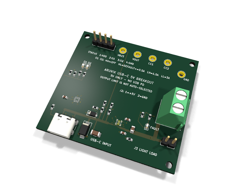
Circuit review & bench-test guide →
Components#
Every placed component, with the reason it is on the board. Extracted directly from the schematic, so this cannot drift from the design.
| Ref | Value | What it does on this board | Part number | Footprint |
|---|---|---|---|---|
C1 |
4.7uF 50V X7R | — | — | C_1206_3216Metric |
C2 |
100nF 10V X7R | — | — | C_0603_1608Metric |
C3 |
330pF 50V C0G dVdt | — | — | C_0603_1608Metric |
C4 |
2.2nF 50V C0G ITIMER | — | — | C_0603_1608Metric |
C5 |
10uF 10V X7R | — | — | C_0805_2012Metric |
D1 |
BAT54H,115 | — | — | D_SOD-123F |
D2 |
OUT1 AMBER | — | — | LED_0603_1608Metric |
D3 |
OUT2 AMBER | — | — | LED_0603_1608Metric |
D4 |
FAULT RED | — | — | LED_0603_1608Metric |
D5 |
SMAJ5.0CA | — | — | D_SMA |
J1 |
USB4105-GF-A-120 | — | — Datasheet ↗ |
USB_C_Receptacle_GCT_USB4105-xx-A_16P_TopMnt_Horizontal |
J2 |
POWER OUT | — | — | TerminalBlock_Phoenix_MKDS-1,5-2-5.08_1x02_P5.08mm_Horizontal |
J3 |
BREADBOARD OUT (LIGHT LOAD) | — | — | PinHeader_1x02_P2.54mm_Vertical |
J4 |
STATUS | — | — | PinHeader_1x04_P2.54mm_Vertical |
R1 |
900k 1% | — | — | R_0603_1608Metric |
R2 |
47k | — | — | R_0603_1608Metric |
R3 |
47k | — | — | R_0603_1608Metric |
R4 |
3.3k | — | — | R_0603_1608Metric |
R5 |
3.3k | — | — | R_0603_1608Metric |
R6 |
215k 1% | — | — | R_0603_1608Metric |
R7 |
100k 1% | — | — | R_0603_1608Metric |
R8 |
374k 1% | — | — | R_0603_1608Metric |
R9 |
100k 1% | — | — | R_0603_1608Metric |
R10 |
976R 1% (3.4A nominal) | — | — | R_0603_1608Metric |
R11 |
47k | — | — | R_0603_1608Metric |
R12 |
3.3k | — | — | R_0603_1608Metric |
R13 |
0R SHIELD LINK | — | — | R_0603_1608Metric |
TP1 |
VBUS_RAW | — | — | TestPoint_Plated_Hole_D2.0mm |
TP2 |
VOUT_5V | — | — | TestPoint_Plated_Hole_D2.0mm |
TP3 |
CC1 | — | — | TestPoint_Plated_Hole_D2.0mm |
TP4 |
CC2 | — | — | TestPoint_Plated_Hole_D2.0mm |
TP5 |
GND | — | — | TestPoint_Plated_Hole_D2.0mm |
U1 |
TUSB320LAI | — | — Datasheet ↗ |
Texas_X2QFN-12_1.6x1.6mm_P0.4mm |
U2 |
TPS259470A | TI TPS25947 RPW0010A 10-pin VQFN-HR land pattern | — Datasheet ↗ |
Texas_RPW0010A_VQFN-HR-10_2x2mm_P0.45mm |
Signals#
Net labels used in the schematic, which are also the names the HDL top level should use.
CC1 CC2 EFUSE_FLT_N EN_UVLO GND OUT1 OUT2 OVLO VBUS_RAW VDD_5V VOUT_5V
Production status#
| Schematic ERC | 0 violations |
|---|---|
| PCB layout | complete |
| DRC | 1 violations |
| Fab package | not exported |
| Fabricated | no — design stage only |
Source: boards/usb-c-5v-breakout
Purpose#
A small power-only USB Type-C sink board that exposes the source's initial 5 V VBUS supply and reports whether the source advertises default, 1.5 A, or 3 A Type-C current. It does not perform USB Power Delivery negotiation and cannot request 9 V, 12 V, 15 V, 20 V, or a PPS voltage.
Proposed electrical design#
J1: GCT USB4105-GF-A-120 USB 2.0 Type-C receptacle (16 contacts, top mount, 1.20 mm shell stakes).U1: TI TUSB320LAI Type-C port controller in GPIO/UFP mode. It provides the requiredRdterminations and detects the source's advertised current.R1: 900 kOhm, 1%, VBUS toU1.VBUS_DET, as required for UFP operation.J4: logic/status header exposingOUT1,OUT2, VDD, and GND. Attachment and current mode are decoded fromOUT1/OUT2.- Two status LEDs mirror the open-drain
OUT1/OUT2pins; the silkscreen carries the decode table below. U2: TI TPS259470A eFuse. The initial configuration provides active current limiting, controlled inrush, adjustable UVLO/OVLO, fault indication, and true reverse-current blocking. The limit-setting resistor targets 3.0 A nominal.D5: SMAJ5.0CA bidirectional TVS on raw VBUS; final clamping behavior must be verified with the connector/cable inductance and the eFuse absolute maximum rating.D1: Schottky isolation between raw VBUS and the VBUS-powered TUSB320LAI.C1: 4.7 uF, 50 V X7R VBUS input capacitor in 1206. The nominal and positive-tolerance value remains below the 10 uF Type-C sink limit, while the larger voltage/package margin makes retaining at least 1 uF at 5.25 V practical. The exact-part typical curve has been reviewed; obtain a current approval sheet or other guaranteed lot data before production.J2: Phoenix Contact 1715721-compatible 5.08 mm fixed screw terminal exposing+5VandGNDfor the power path.J3: optional 2.54 mm header exposing+5VandGNDfor breadboard use at light load only.- Optional test points on VBUS, CC1, CC2, and GND.
- D+/D- and SBU pins remain unconnected; this is a power-only board.
- The connector shell is tied to board ground by a configurable EMI network (default: 0 Ohm link, with optional capacitor footprint).
CC1 and CC2 connect separately to U1; they must not be shorted together. This prototype routes them directly to the controller without a dedicated external IEC-rated CC protector. Connector ESD and CC-short-to-VBUS testing is therefore a release gate; add a low-capacitance protection device if the target end-product immunity cannot be met.
Advertised-current decode#
In the selected GPIO/UFP configuration, OUT1 and OUT2 are open-drain:
| OUT1 | OUT2 | State |
|---|---|---|
| High | High | Unattached |
| High | Low | Attached, default USB current (limit this USB 2.0/power-only board to 500 mA) |
| Low | High | Attached, 1.5 A advertised |
| Low | Low | Attached, 3.0 A advertised |
Important current limitation#
The protection path can carry up to 3 A, but TUSB320LAI detects rather than enforces the advertised limit. The downstream load must obey OUT1/OUT2:
- default indication: limit this USB 2.0/power-only board to 500 mA;
- medium indication: up to 1.5 A;
- high indication: up to 3.0 A.
The connector and copper being rated for 3 A does not grant permission to draw 3 A from every USB-C source.
The TPS259470A current-limit resistor sets approximately 3.4 A nominal. The 976-ohm, 1% value targets about 3.0 A at the low current-limit tolerance corner, so a compliant 3 A load does not nuisance-limit. This protection threshold is not a Type-C current entitlement: the attached load must still obey the lower of the source advertisement and 3 A.
Output interface decision#
Both footprints will be provided in parallel:
- 5.08 mm fixed screw terminal block for load and thermal testing;
- optional 2-pin 2.54 mm header for low-current breadboard experiments.
Do not route 3 A through a solderless breadboard.
Assembly note: this revision uses through-hole footprints for the output terminal block, pin headers, plated test points, and mounting holes. It is suitable for a mixed-technology build or hand-installed output hardware. If the fabrication target is pure SMT automated assembly, replace J2, J3, J4, and the plated test-point footprints with SMT equivalents before ordering.
Layout constraints#
- Keep
U1close to the receptacle and route CC1/CC2 directly without stubs. - Use a short, wide VBUS path from the receptacle through the eFuse to the output connector.
- Stitch the connector shell and ground return with multiple vias.
- Put the TVS at the connector side of the protected power path.
- Preserve the USB4105 board-edge and mechanical keepout requirements from the manufacturer drawing.
PCB layout and fabrication status#
- PCB file:
usb-c-5v-breakout.kicad_pcb. - Reproducible layout generator:
generate_pcb.py. - Stackup: 4 copper layers (
F.Cu,In1.Cu,In2.Cu,B.Cu). - Minimum routed rule set used by this revision: 0.10 mm clearance, 0.10 mm minimum track, 0.45 mm via diameter, 0.20 mm via drill, and 0.15 mm hole clearance / hole-to-hole clearance.
- KiCad ERC: 0 errors and 0 warnings. Strict PCB DRC, including zone refill and schematic parity: 0 electrical/geometric violations, 0 unconnected pads, and 0 parity issues. KiCad retains one non-electrical warning because U2 is a local copy of the custom project footprint; the land pattern is independently checked against TI's RPW0010A drawing. Reports are in
reports/. - Fabrication outputs are under
fab/: fab/gerbers/for Gerbers and Gerber job file;fab/drill/for Excellon drill, drill map, and drill report;fab/assembly/for BOM copy and pick-and-place CSV;fab/review/for top, bottom, and internal-layer SVG review plots;fab/usb-c-5v-breakout.d356for the IPC-D-356 electrical netlist;fab/board-statistics.rptfor stackup, area, drill, and feature statistics.- Rebuild the complete fabrication/assembly set with
python3 fab/generate_outputs.pyafter every released PCB change. - Plated and non-plated holes are exported as separate drill files.
bom/qualified-bom.csvrecords proposed orderable MPNs and SMT-only versus mixed-technology assembly variants.reports/validation-report.htmlis the detailed automated QA and certification-readiness report.- Validate the generated HTML, evidence links, status counts, and certification disclaimer with
python3 qa/validate_report.py.
USB4105 footprint review#
The selected footprint is KiCad's GCT-specific Connector_USB:USB_C_Receptacle_GCT_USB4105-xx-A_16P_TopMnt_Horizontal, used with USB4105-GF-A-120.
GCT's product page identifies the USB4105 as a 16-contact USB Type-C receptacle/socket, USB 2.0, horizontal, surface-mount, top-mount connector with through-hole shell stakes and locating pegs. The same page lists the VBUS pin group at 5 A and the GND pin group at 6.25 A, so the connector rating is not the limiting item for the 3 A target.
The official GCT B4 drawing was checked directly. The footprint matches the recommended component-side layout, including the 0.30 mm signal pads, 0.60 mm power/ground pads, 0.65 mm locating holes, shell-stake geometry, and the 3.68 mm connector-origin-to-board-edge datum. The selected -120 variant uses 1.20 mm shell stakes.
Power-path review notes#
- The protected high-current path uses the USB-C VBUS pins, the TPS259470A eFuse, and the terminal-block output
J2. - The route uses wide copper where the connector and eFuse geometry allows, with short unavoidable neck-downs at the USB-C contacts and the TPS259470A IN/OUT pads.
J2is the intended load-test output for high-current use.J3is only for low-current breadboard experiments.C3is 330 pF C0G and targets an approximately 1 ms eFuse ramp;C5is the initial 10 uF output capacitance. The faster ramp reduces linear-region stress when a load is present at attachment while keeping capacitive inrush modest. Final behavior must be verified on hardware with the intended cable, source, and load.C1is 4.7 uF nominal. Its +10% tolerance corner is 5.17 uF, below the 10 uF Type-C UFP maximum. To remain above 1 uF after -10% tolerance and the X7R temperature corner, the selected part must retain at least 27.8% of its nominal capacitance at 5.25 V DC bias. Murata's exact-part typical curve retains well above 90% there, but the chart is not a guaranteed limit; obtain a current approval sheet or guaranteed lot data before production.- Thermal behavior is layout-reviewed only. Before production, run a 3 A continuous-load temperature-rise test and check the eFuse package, USB-C connector, terminal block, and VBUS/VOUT copper near the package neck-downs.
Simulation#
A standalone behavioral simulation harness is available in sim/. It includes ngspice testbenches and a Python runner covering 5 V hot-plug, 0.1 A to 3 A load step, short-circuit, and reverse-backfeed scenarios. The model is an early board-level approximation and does not replace TPS259470A fault-timer, thermal, or hardware validation.
Design review checklist#
- [x] Target a 3 A-capable path and add advertised-current detection.
- [x] Provide terminal-block and optional breadboard-header outputs.
- [x] Select TUSB320LAI GPIO/UFP current detection.
- [x] Select TPS259470A as the protected load-switch/eFuse.
- [x] Draft the complete schematic and annotate initial part numbers/values.
- [x] Save the imported capture as native KiCad 10
.kicad_sch. - [x] Run KiCad 10 ERC with zero violations.
- [x] Create the TI RPW0010A eFuse footprint from manufacturer land-pattern drawing 4225183/A.
- [x] Cross-check the selected GCT-specific USB4105 footprint against the official GCT B4 drawing, product specification, and current ratings.
- [x] Complete PCB layout and run DRC.
- [x] Review inrush/capacitance, thermal risks, and the 3 A copper path at layout level.
- [ ] Bench-validate inrush waveform, current-limit behavior, and thermal rise at 3 A on prototype hardware.
- [x] Generate and inspect fabrication outputs.
- [x] Run strict schematic-to-PCB parity, BOM/PnP parity, analytical corner checks, simulation assertions, and fabrication-manifest checks.
Primary references#
- GCT USB4105 product page: <https://gct.co/connector/usb4105>.
- TI TUSB320LAI datasheet.
- TI TPS25947 family datasheet.
- Murata GRM31CR71H475KA12L exact-part product/characteristic data.
- USB Type-C specification for sink
Rd, attach behavior, and current limits.